Hardware Testing
Testing Requirements
Particularly when building the hardware yourself, we recommend a test procedure that we established for our own builds. These tests can be done without knowing much of the hardware details. For a better understanding, take a look at the hardware concept, though.
If you use professionally assembled boards, you can skip many steps in the test, as soldering errors are relatively uncommon as compared to hand soldering.
For executing the tests, you need the following tools and should be experienced in their use:
- Power supply (12V with current limitation)
- Multimeter
- Oscilloscope (2 channels)
- Signal generator
- Assembled ahoi testboard
For the extended / automatic tests:
- Working mainboard with firmware
- Tiepie oscilloscope (2 inputs, 1 signal generator output; e.g. the HandyScope HS5)
In the following, we describe standard test procedures for each board. The boards can be tested alone or together with a mainboard, which of course requires a tested and working mainboard.
TXB
Manual test
- For a test without a connected mainboard, an externally generated signal must be used. The DAC has to be disconnected by removing resistor JS.
Danger
Failure to remove JS in the following test procedure will apply a reverse voltage to the DAC and may cause permanent damage.
-
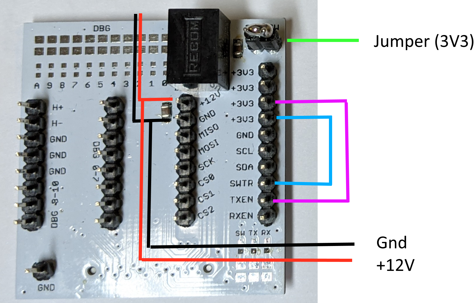
Use a testboard (AHOI-TST) to generate the logic-level voltage and to enable the TXB board. On the testboard, connect the 3.3V Jumper (green). Connect 12VDC (red) and GND (black) to a power supply. Attach the testboard to the TXB board. Leave the blue and pink connection open, they will be connected later.
The power consumption (at 12V) should be around 4.5 mA.
-
Connect TXEN to 3.3V (pink). Power consumption should increase to around 70–80mA (7-8mA, if only the DCDC supplies without amplifiers are soldered on the TXB board). You should see a stable and symmetrical voltage around +- 22VDC at the testpoints V+ and V-, respectively. Depending on the resistor tolerances, a few hundred millivolts of error are expected and acceptable.
Voltage
Maximum rating for the components in the power path (connected to V+ and V-) is +-30V, exceeding these values will damage the components.
note
The positive regulator (DCDCP) may operate in an unstable state, in which the IC draws a high current and can get damaged! Connect TXEN only after the 3.3V (of the test board) is stable.
-
Connect a signal generator to the test pad "Input". Configure the device to create a sine wave with 3.0V peak-to-peak amplitude, an offset of +1.5V, and a frequency close to the center frequency of your communication band (typically around 42kHz). Use the common ground (on the test board) as signal ground.
An amplified output signal (Amplitude 10.2V, no offset) can be measured at the test points A and B. The phase difference between both signals should be around 180°.
-
Connect SWTR on the testboard to 3.3V (blue). The output of the TXB power amplifier is now connected to the hydrophone output. Connect two channels of an oscilloscope to the pin headers "H+" and "H-" on the test board; yoo should then see a signal similar to the one in the following picture:
")
The green curve is the inverted hydrophone output (H-), the yellow one the non-inverted output (H+). The input signal is blue, and the signal after the gain stage is pink. In our test, we used a frequency of 60kHz.
Please note that the gain stage will default to a gain of 0.5; therefore, the peak-to-peak amplitude at the transmitter board outputs H+ and H- will be half of the maximum.
If you experience different voltages at the transmitter output, we suggest to check the signal path at the following intermediate test points:
- The peak-to-peak amplitude at the low-pass filter outputs L1 and L2 should be 3V with an offset of 1.5V.
- The peak-to-peak amplitude at the gain stage G should be 1.5V with an offset of 1.5V.
- The peak-to-peak amplitudes of the power amplifier stage (A and B) should be 20V with a 0V offset and a 180° phase shift.
- The peak-to-peak amplitudes of the output signals (H+ and H-) should be the same as A and B.
Test with Mainboard
For a test with the mainboard, you need a working MoSh (see setup PyLib) and a USB to UART converter (3.3V logic-level).
The DAC has to be connected to the amplifier, so the resistor JS must be soldered (if not already).
Input to the shell is marked with >>.
-
Attach the TXB board to the mainboard. Connect a power supply (12V) to the supply pins of the mainboard (12V, GND). Connect the mainboard to your PC via the USB to UART converter and the hydrophone output of the TXB board to an oscilloscope. The oscilloscope should be configured as follows:
Parameter Setting Horizontal 30ms / div Vertical (amplifier output) 10V / div Vertical (testpoint IN) 3V / div Trigger rising edge, 1V -
Open the MoSh in a terminal. If asked, select the correct serial port.
-
To check the connection with the modem, type the 'id' command. You should see an answer like this (or similar):
>> id TX@1603887394.186 00 FF 84 00 00 00 RX@1603887394.201 00 00 84 00 00 01 00 () -
Set the output of the TXB to its maximum value by choosing TX gain level zero. Each step increases the attenuation by 3dB.
>> txgain 0 -
Send the command to generate a test sweep. The first parameter "false" disables the compensation for a specific hydrophone transmission curve. The second parameter is the gap between the frequencies as number of symbols.
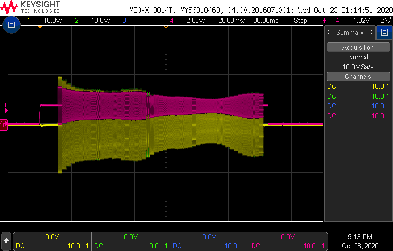
>> testsweep false 1The output waveforms should look like the following pictures (left). The amplitude of the DAC signal (red) is 3V, the amplitude of the amplifier output 22V.
Each bar is a specific transmission frequency and should have an identical amplitude (like the left picture).
The right picture shows the signal with active hydrophone transmission curve compensation and no delay between each frequency. This makes it harder to detect a fault in the transmission.
Compensation off, single delay Compensation on, no delay testsweep false 1testsweep true 0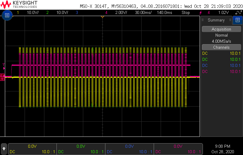
-
Repeat steps 4 and 5 with increased attenuation, i.e.:
>> txgain 2
>> testsweep false 1
The waveform should look like the previous one, but the amplitude should be reduced by 6dB (50%).
Testpoints
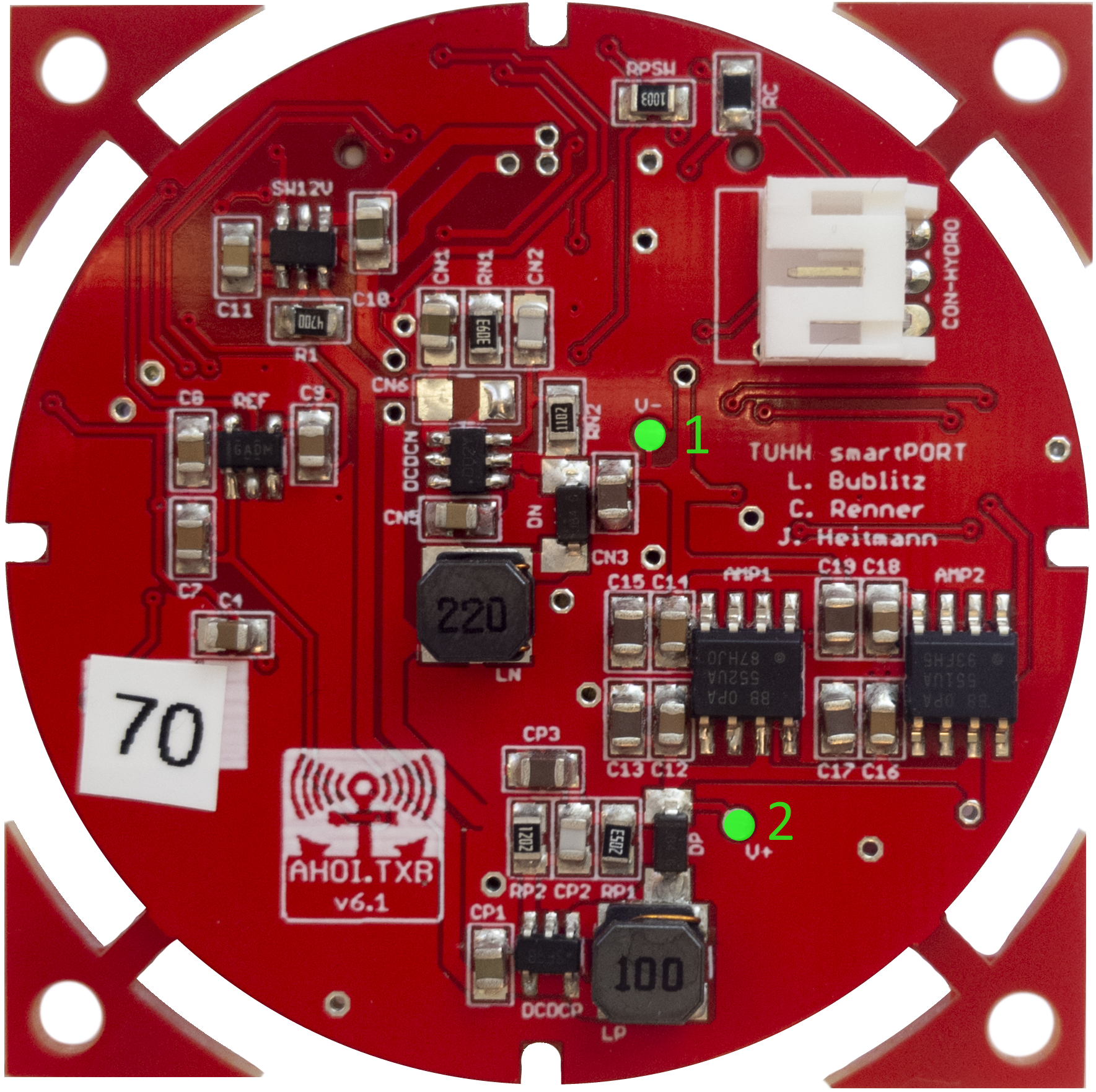
If some part of the circuit is not working correctly, it is possible to check the single stages of the amplification. The testpoint locations are marked in green in the following pictures.
| Top | Bottom |
|---|---|
 |
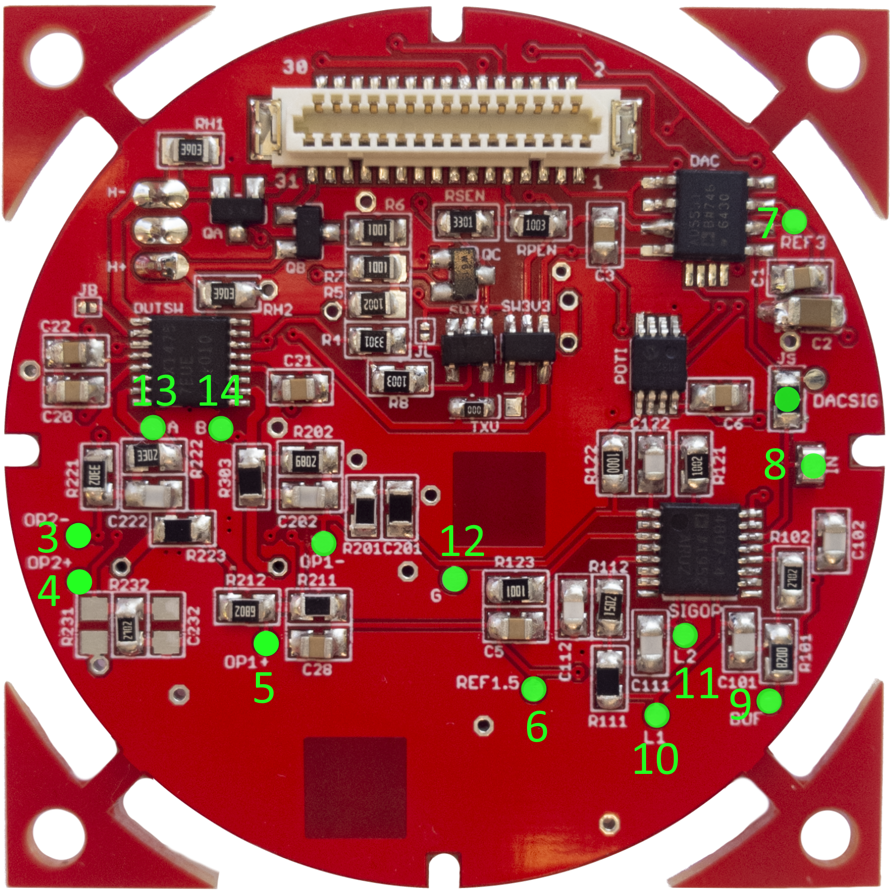 |
| Location | Testpoint | Description | Signal |
|---|---|---|---|
| 1 | V- | Supply amplifier | -22V |
| 2 | V+ | Supply amplifier | +22V |
| 3 | OP2- | Feedback OP2 -> A | 0,5 * A + 0,5 * B |
| 4 | OP2+ | Feedback OP2 -> A | 0V |
| 5 | OP1- | Feedback OP1 -> B | B / 27 |
| 6 | REF1.5 | Voltage reference | 1.5V |
| 7 | REF3 | Voltage reference | 3.0V |
| 8 | IN | Input for test signal | --- |
| 9 | BUF | Signal after buffer | Input (IN) |
| 10 | L2 | Signal after LP1 | Input (IN) |
| 11 | L1 | Signal after LP2 | Input (IN) |
| 12 | G | Signal after gain control | G * Input (IN), (G = 0.5, if no MB connected, G = -3 |
| 13 | A | Output signal | Output, no DC Offset, 180° between TP A and TP B, 20Vpp |
| 14 | B | Output signal | [See TP A] |
Transmitter (TX)
Test
Info
The TX Board can be tested similar to the TXB board, so only the differences are described in the following.
The resistor RS1 connects the DAC to the amplifier stage. For testing the amplifier stage, resistor RS1 has to be removed and an external signal generator can be connected to the input pad. The TX board is more sensitive than the TXB board and can easily become damaged during tests. Therefore, it is recommended to assemble the whole board, check for shorts and test it directly with the mainboard and RS1 soldered. The TX boards only use the H+ signal of the hydrophone. H- is tied to ground. The peak-to-peak amplitude of the output signal should be around 32V.
Testpoints
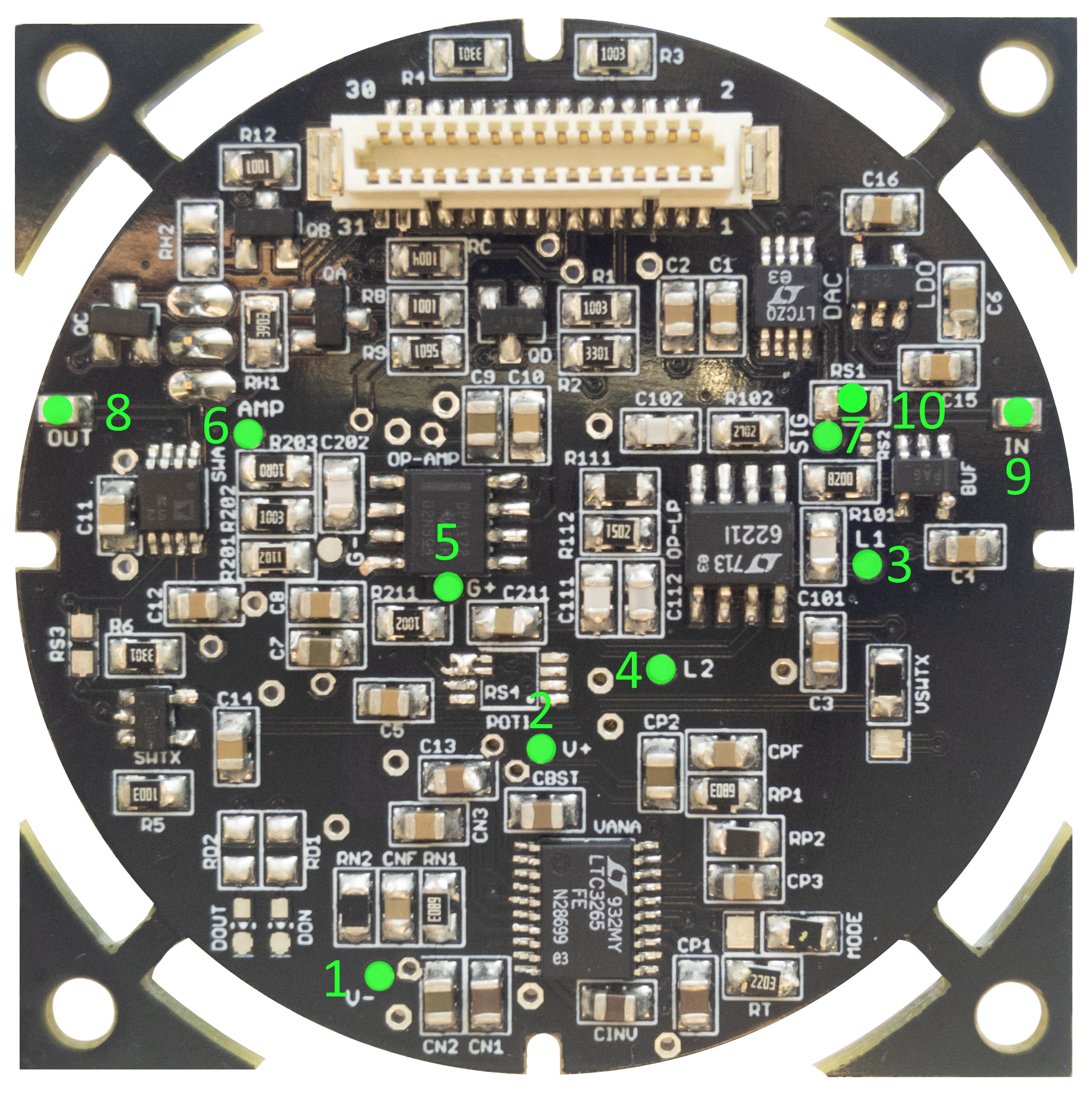
| Location | Testpoint | Description | Signal |
|---|---|---|---|
| 1 | V- | Supply voltage | -18V when TXEN is high |
| 2 | V+ | Supply voltage | +18V when TXEN is high |
| 3 | L1 | Signal after Low-Pass 1 | IN, unmodified in working band |
| 4 | L2 | Signal after Low-Pass 2 | IN, unmodified in working band |
| 5 | G+ | Amplifier positive Input | Attenuated L2 signal, Attenuation configurable |
| 6 | G- | Amplifier negative input / feedback | Input * 10.1 => 32Vpp |
| 7 | AMP | Amplified signal | Input * 10.1 => 32Vpp |
| 8 | SIG | DAC output | DAC Waveform |
| 9 | OUT | Amplified output signal | AMP when SWTX high |
| 10 | IN | Input for amplifier stage | Controlled by DAC if RS0 not soldered => input for test signal |
| 10 | (RS1) | Connects DAC to SIG, remove when IN is used as signal source |
Receiver (RX)
The receiver circuits are designed to amplify extremely small signals. Testing a receiver board requires to attenuate the input signal before they get inserted into the input pins of the RX circuit. For the following tests, you need the following attenuation circuit, where the value RA of resistor R1 differs between test procedures.

If required: Connect the ground of the signal generator to the ground of the 12V supply near the connector on the testboard. If the ground of the signal generator is internally tied to the ground of the oscilloscope, we strongly advise to not connect the signal generator ground to prevent ground loops.
Only AC input signals
The input stage (JFET) will be damaged if a DC signal is applied. Never connect a signal generator directly to the receiver board. Make sure that the generated signal only contains AC components.
Manual test
A manual test of the receiver board can be done by applying a signal at the hydrophone input pins and measure the amplified signal at the ADC input pins. To get access to the hydrophone pins use the ahoi test board.
-
Choose RA = 10 k\(\Omega\) (attenuation of 1,000x)
-
Attach the ahoi test board to the RX board. Connect the 12V supply pins to a 12V power supply. Make sure that the 3.3V supply jumper is connected. The current should be around 4.6mA (caused by the DCDC converter on the testboard).
-
Connect RX_EN to 3.3V on the test board. The current should increase to ca. 15mA.
-
Check the voltages on the board (see Testpoints).
-
Apply an input signal to the hydrophone pins. Use the following settings: 2V peak-to-peak amplitude, zero DC offset, 42 kHz.
-
Measure the output signals (see testpoints). At testpoint SIG, you should measure a signal with an amplitude of around 4V. (Pre: ca. 15mV, Pre2: ca 900mV).
Automatic test
The receiver board can be tested with an automated test procedure and setup (shown in the following picture). This procedure will measure the frequency response of the bandpass across a wide frequency range and lets you see if the analog filter chain and gain adjustment is working correctly.
You have to attach a mainboard with a USB to UART converter to the RX board. For the measurements, a Tiepie USB-oscilloscope is used (HandyScope HS5). The generator output is used as the signal source connected to input 1 of the oscilloscope (to check if the generator signal is correct) and the attenuator circuit. The attenuated signal is connected to the RX board via the programming board (figure 8). Use the pins at the red marking.
Connect the power supply to the 12V connector on the mainboard. Only connect the ground of input 2 of the Tiepie oscilloscope to the ground at this connector. Leave the other ground connectors of the Tiepie unconnected.

Proper wiring and hardware setup
In this setup, the following aspects are important to obtain proper results:
- Use shielded connections from the input voltage divider to the modem inputs (H+ and H-)
- Only connect the ground of the second HS5 channel to ground, leave the grounds of the signal generator and channel 1 floating
- Use a 10,000x voltage divider (RA = 100k\(\Omega\)) - confirm the values of the voltage divider resistors to be within 1%
Note that the voltage divider in this setup differs from the one required for the manual test!
After you have set up the hardware, it is necessary to set up the software.
The required scripts can be found in the ahoi-tools repository (see Git Repositories). Follow the instructions in the included INSTALL file (pcb-test tiepie/). A working modem PyLib is also necessary. If it's not set up already, do it now.
Afterwards, start the automatic measurement script:
>> python3 pcb-test/tiepie/recRXGain.py id
The result of the measurements will be saved in the folder data. Replace 'id' with the number under which you want to store the files. We encourage you to label all boards with a numeric ID. After starting the script, you have to select the serial port, which is used for communication with the mainboard. The following output should appear on the screen):
setting  1 of  4, gain level:  0
Vs =    8, gain =   844 (58.5 dB)
<libtiepie.oscilloscope.Oscilloscope object at 0x0000018CFC0A6F40>
<libtiepie.generator.Generator object at 0x0000018CFEE52BB0>

RUN 1 of 1
f =       0 ...............................
f =   12000 ...............................
f =   24000 ...............................
f =   36000 ...............................
f =   48000 ...............................
f =   60000 ...............................
f =   72000 ...............................
f =   84000 ...............................
f =  102000 ...............................
f =  294000 .........................
saving ...
View the data
When the measurements are complete, they can be evaluated with
>> python3 pcb-test/tiepie/evaRXGain.py id
gain  0:  mean = 2.498V, std =   6.7mV
gain  6:  mean = 2.499V, std =  14.3mV
gain 12:  mean = 2.501V, std =  48.0mV
gain 18:  mean = 2.501V, std = 243.2mV
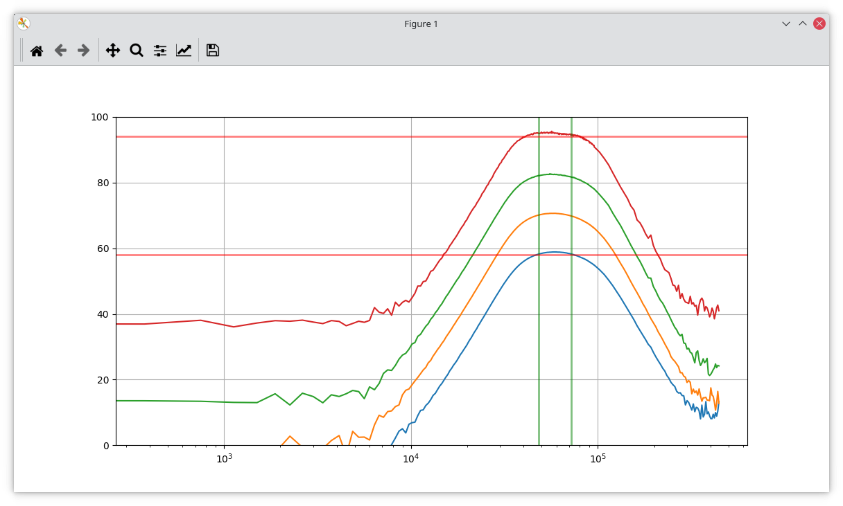
This output shows the mean voltage and standard deviation of the filtered and amplified signal for different gain levels. The mean voltage should be close to 2.5V (with an error of at most 10mV). The standard deviation should fall in the shown orders of magnitude, where it should approximately quadruple from output row to row. As a rule of thumb, the standard deviation in gain level 18 should be in the range of 100mV and 300mV; if not, there probably is an error in the signal chain of the receiver board.
The created plot, see the example below, shows the gain (y-level, in dB) of four gain levels (0, 6, 12, 18) over a frequency range (x-axis, in Hz). The communication band (bandpass region) is marked by two green vertical lines. The red horizontal lines indicate the desired gain for the lowest (0) and highest (18) gain level inside the communication band. The top curve (red in the example) should be close (within 1 or 2dB) to the upper desired gain level. The bottom curve (blue in the example) should be close (within 1 or 2dB) to the lower desired gain level. The other two curves should be evenly spaced in between. All curves should roll-off symmetrically around the passband and similar to the ones in the example.
Extended measurements
To speed up the testing procedure, the test script only measures the frequency response of the receiver for four gain levels by default. It is, however, possible to measure additional gain levels with the option -l:
>> python3 recRXGain.py <id> -l start:step:stop
This will measure the frequency response (gain) from level start to stop with a step size of step.
For further analyze, we would like to point out that the recorded data will be stored in the folder pcb-test/tiepie/data/rx-id as Matlab files.
Testpoints
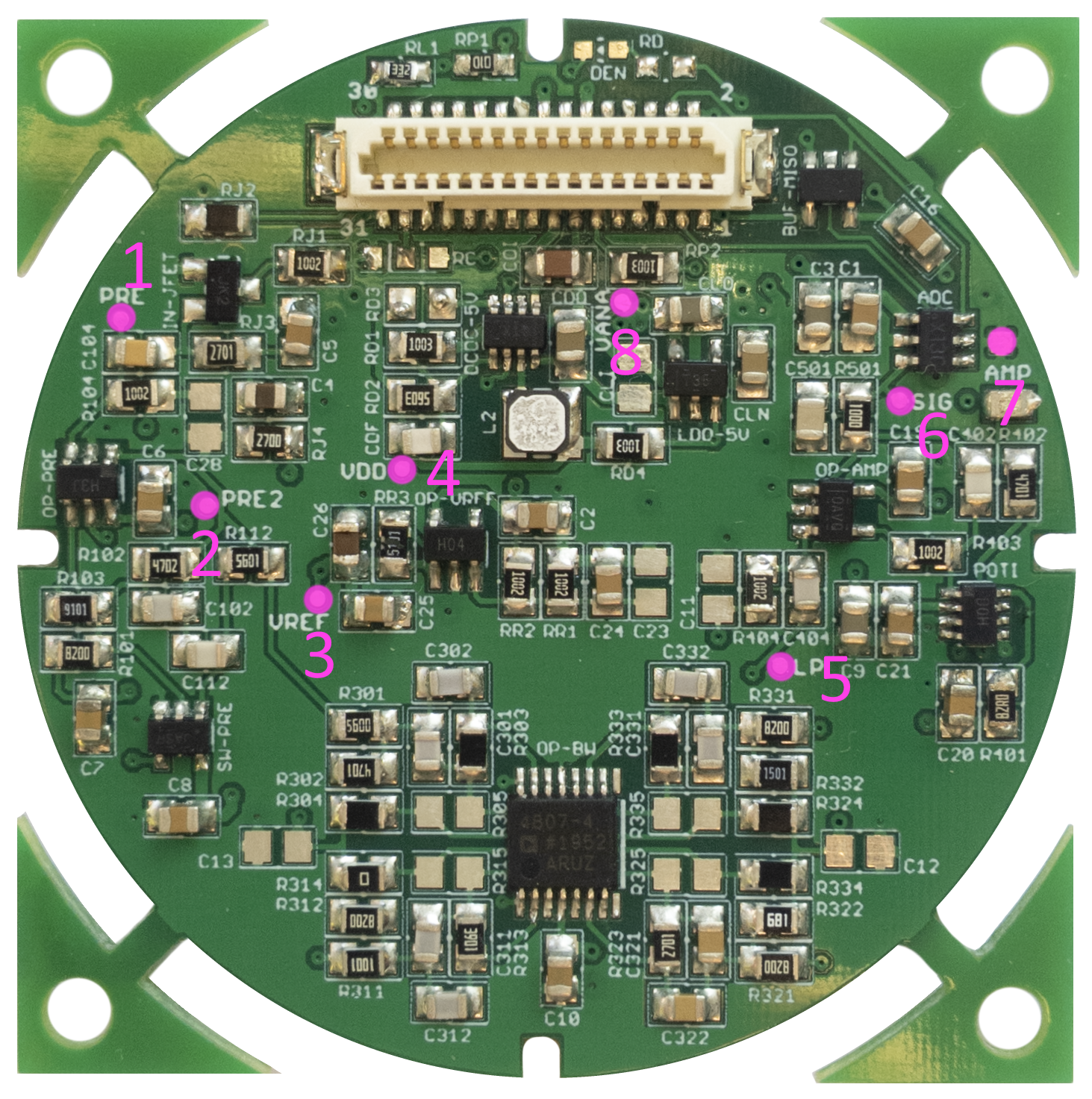
| Location | Testpoint | Description | Signal |
|---|---|---|---|
| 1 | PRE | Signal after pre-amplifier 1 (fet) | H. Input * 7.5 |
| 2 | PRE2 | Signal after pre-amplifier 2 (opamp) | PRE * 60 |
| 3 | VREF | Reference voltage for op-amps | VANA / 2 => 2.5V |
| 4 | VDD | Supply voltage | ~5.25V when RXEN high |
| 5 | LP | Signal after 8th order bandpass filter | PRE2 * 1.5 (42kHz) |
| 7 | AMP | LP * Gain (Poti) 1 | |
| 6 | SIG | ADC input (AMP plus buffer RC) | AMP |
| 8 | VANA | Switched supply voltage | 5.0V when VDD power good |
If the bandpass filter is not working correctly, further points are available for testing:
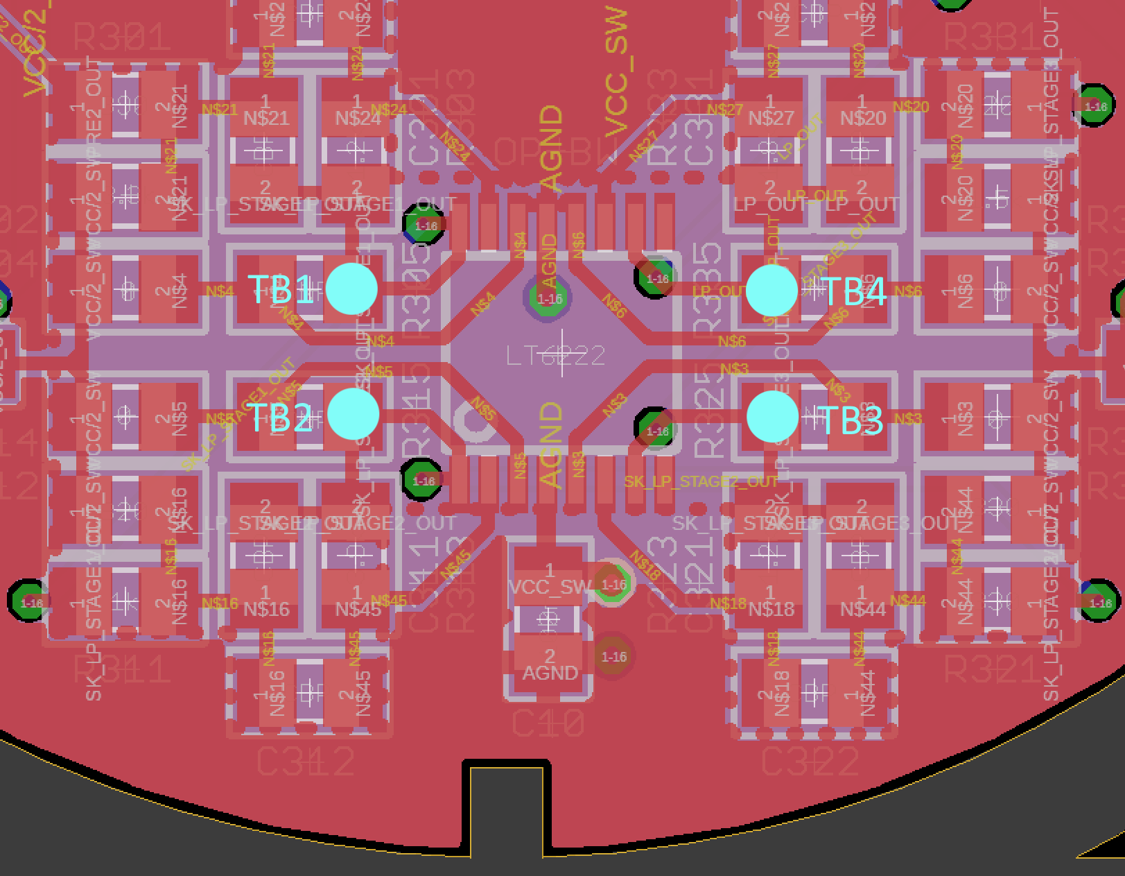
| Testpoint | Gain | Source |
|---|---|---|
| TB1 | ca. 1.5 | PRE2 |
| TB2 | ca. 1 | TB1 |
| TB3 | ca. 1 (-5%) | TB2 |
| TB4 / LP | ca. 1 (+5%) | TB3 |
Mainboard (MB)
Test
The mainboard has no dedicated test points. All circuit parts work independently of each other. If some part of the board is not working correctly, you can use the schematic to check the components for their function.
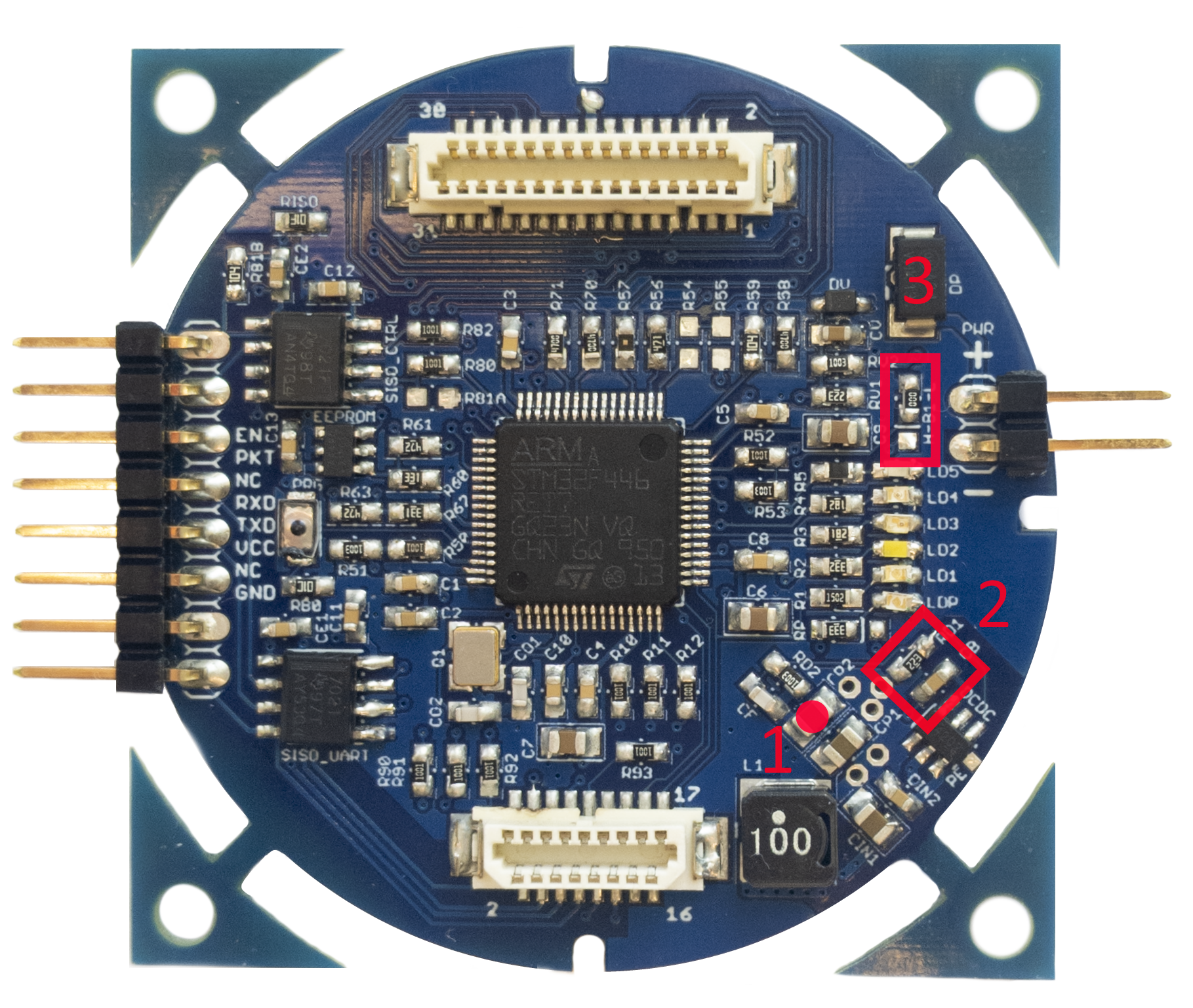
One central part of the board is the power supply circuit. It is used to create the 3.3V from the input voltage, distribute it to the components on the mainboard and - via the connectors - to the daughter boards (RX, TX/TXB). If this is not working correctly, it can damage many components and should be tested before the following components are soldered: microcontroller, EEPROM, isolators. The 3.3V should be measurable on the capacitor located at position 1 (following picture).
If there is no voltage, check the DCDC converter (IC, inductor) and the polarity protection diode. If the voltage is too high, make sure that the feedback network at position 2 is soldered properly and the coil is not shorted. After you have checked the voltage and soldered all components, the mainboards need to be programmed with the firmware (see chapter: flashing the modem).
Testpoints
-
Gain in unconfigured state: x3 ↩