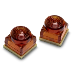
Design of a PCB and Evaluation of the OWC Transceiver AFBR-FS13B25
- Typ der Arbeit: Forschungsprojekt
- Status der Arbeit: offen
- Projekte: SatelLight
- Betreuer: Marek Jahnke
Before continuing please visit: Project Thesis
In this project work the Broadcom AFBR-FS13B25 Transceiver for Optical Wireless Communication should be implemented and evaluated.
Motivation
In the SatelLight-Project, the use of LiFi/Optical Wireless Communication for intra-satellite-communication is currently being researched.
The AFBR-FS13B25 OWC Transceiver seems to be a good candidate to be used as a transceiver due to its size, power supply specification and potential bandwidth.
In this project work the AFBR-FS13B25 OWC Transceiver should be integrated and evaluated on a new designed pcb. This enables further demonstration and testing of e.g. MAC protocols or Forward-Error-Correcting (FEC) Techniques in Optical-Wireless-Communication setups. Therefore, the PCB needs to be designed for further use in mind.
An optionally activatable Serializer/Deserializer should be added, to be able to transmit and receive data from a slower (parallel) interface.
To get a first impression, after implementation the transceiver should be demonstrated and evaluated by basic transmission of data.
Tasks
In this project work, the student has to perform the following tasks:
- Familiarization with the topic: Optical Wireless Communication in general, the transceiver chip, high speed/frequency pcb design.
- Design HW
- A PCB is to be designed, that contains the Transceiver and corresponding circuitry.
- It should be designed with optimizations for high frequency and speed in mind.
- The PCB should have suitable interfaces, jumpers and connectors for later further configuration, evaluation and simple use (e.g. TX, RX, Power, Enable, other signals from/to the Transceiver)).
- A serializer/deserializer (serdes) chip has to be used (configurable/activated e.g. by jumpers), to be able to convert and transmit data from a slower parallel interface (e.g. MCU/FPGA GPIOs) to the transceiver and back again on the receiving side.
- An external programmable clock generator might be necessary, to achieve the corresponding clock rate (at Serdes-Interface)
- Search for components.
- Soldering of PCB.
- Evaluating the setup:
- Interfacing and controlling the Transceiver(s) with a MCU or FPGA.
- Testing general use.
- Evaluating performance, data transmission (distance, speed, different environments, with or without ambient light, angles, power consumption).
- Documentation:
- Documenting the project in GitLab.
- Proper circuit design and documentation (KiCad)
- Proper code structure and comprehensible code documentation has to be maintained.
- Report: Documentation, Components, Pin assignments, calculations, reasonings why something is done, submitted as PDF

Further Reading
-
- Visible Light Communication, Networking, and Sensing: A Survey, Potential and Challenges
-
IEEE Communications Surveys &$\mathsemicolon$ Tutorials17.4Institute of Electrical and Electronics Engineers (IEEE)2015.
10.1109/comst.2015.2476474 [BibTex]


